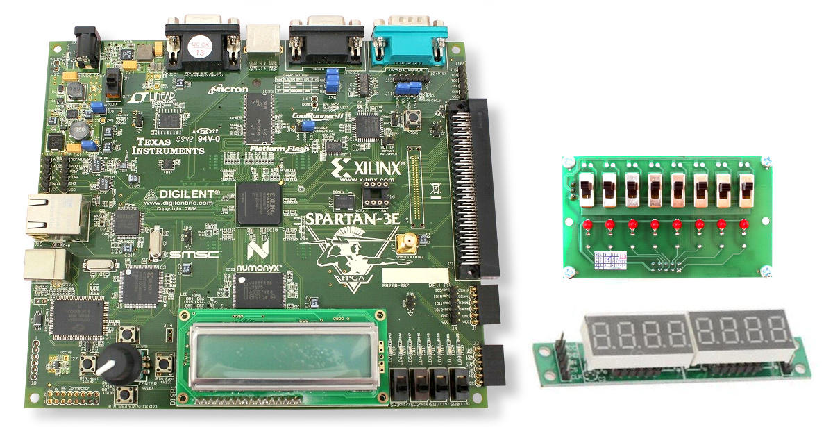
This 8-bit RISC Microcontroller was constructed from individual logic gates and implemented on an FPGA (Field Programmable Gate Array) chip. To test the system, a bank of slide switches and pushbuttons is used to input data and instructions. An alpha-numeric (hexadecimal) display is used to read the Program Counter, the current program instruction or the value of a selected register.
Design:
The proposed Microprocessor architecture has an 8-bit address bus and 16-bit word size (Fig. 1).
The architecture includes a Control Unit, Arithmetic Logic Unit, Instruction Fetcher and a Memory Controller (Fig. 2).
It supports a small Instruction Set based on Atmel and RISC, where each instruction cycle takes 4 or 5 clocks.
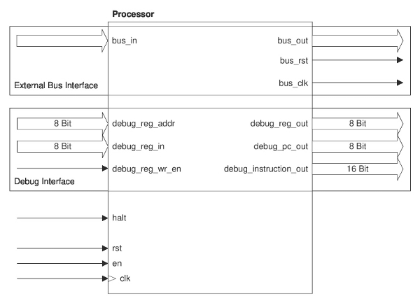 |
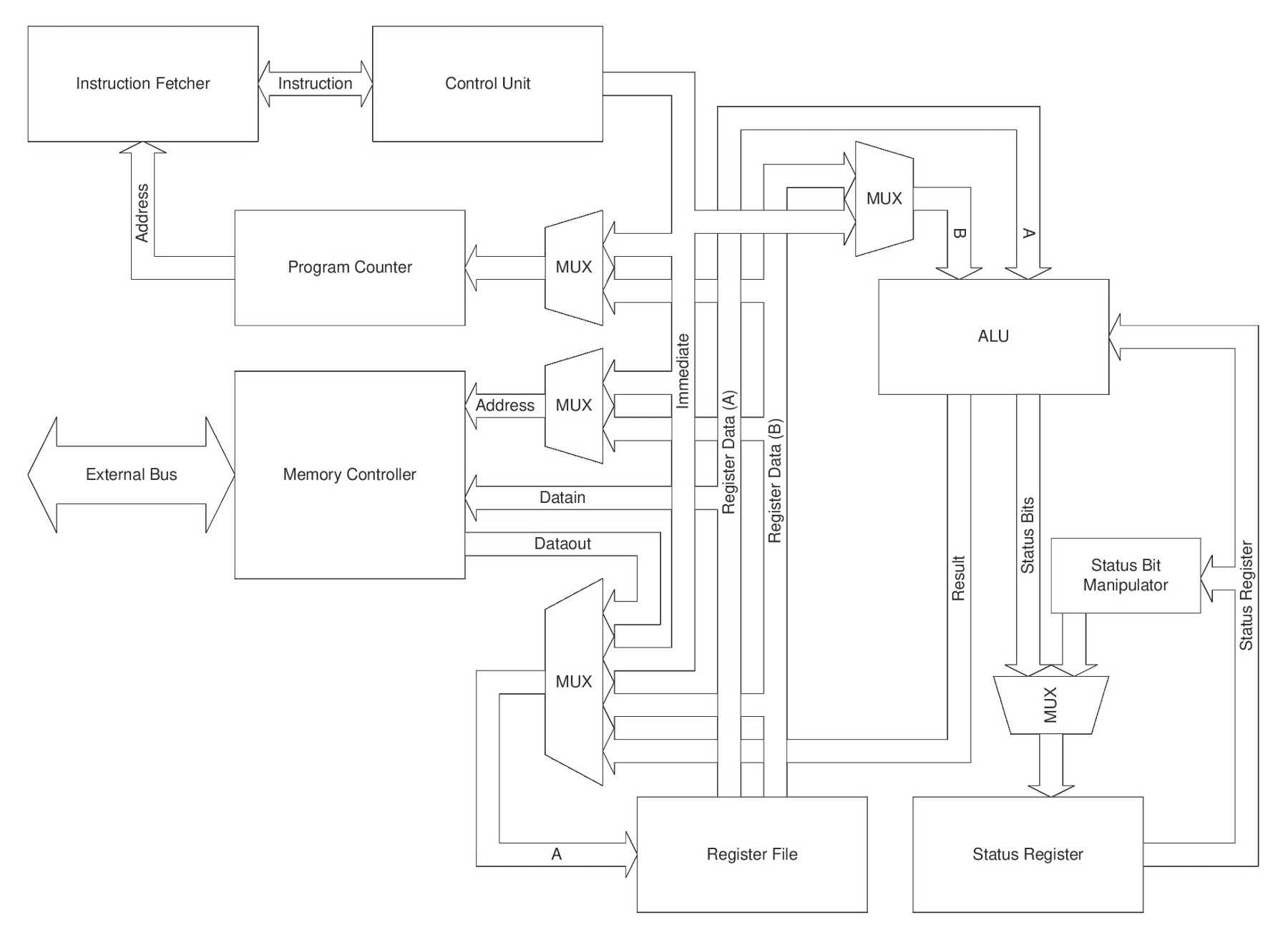 diagram and data path. |
|
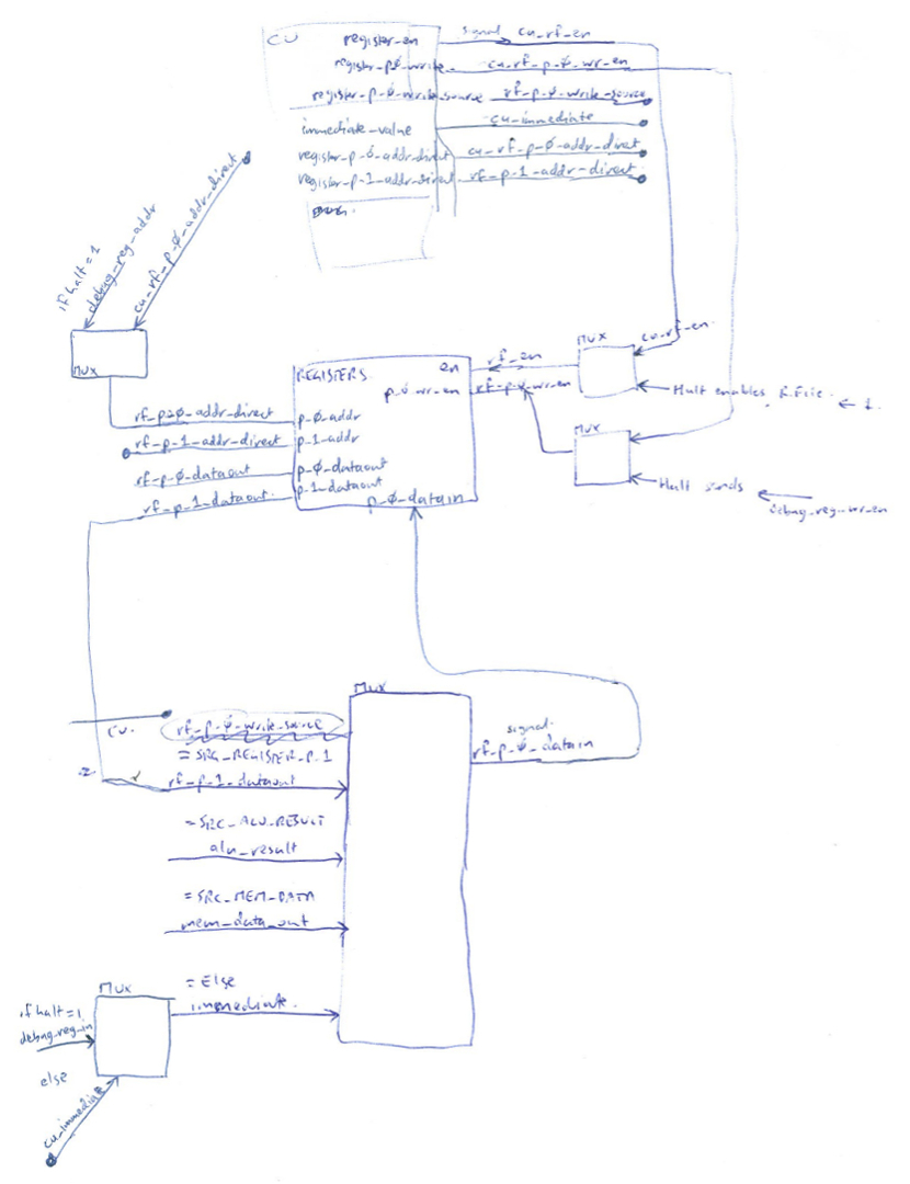 between Control Unit and Registers. |
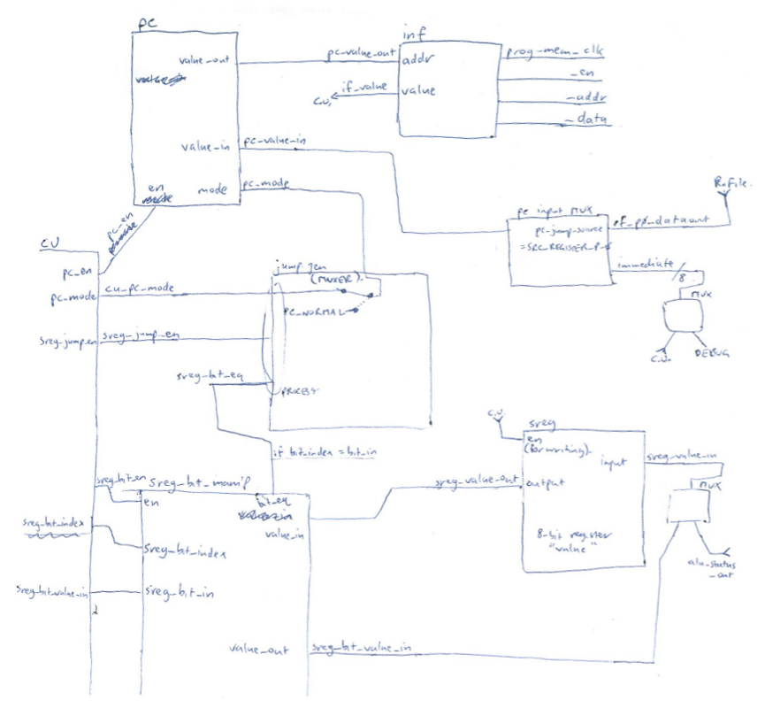 between Control Unit, Program Counter and Jump Generator. |
Implementation:
The design was synthesized in VHDL using Xilinx ISE, analysed and tested in simulation,
then implemented on a Xilinx Spartan3E Development Board.
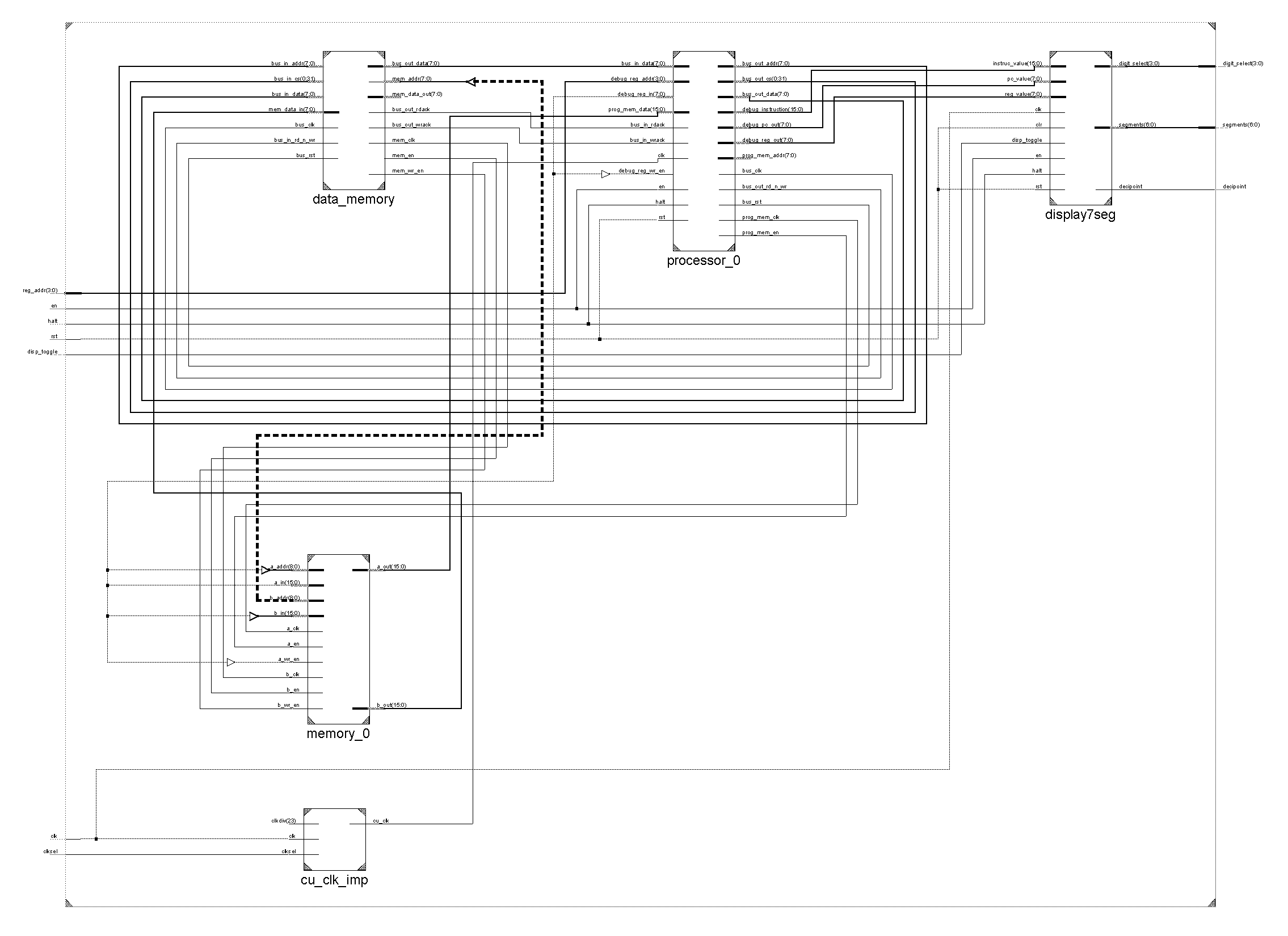 controller (Processor + Memory). |
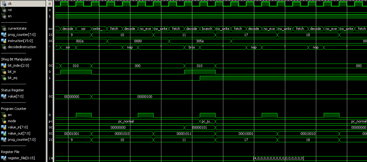 testing Microcontroller in simulation. |
 |